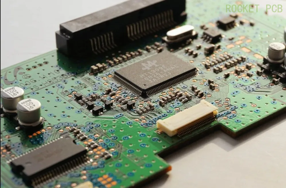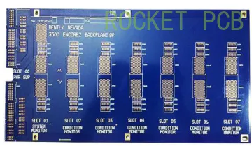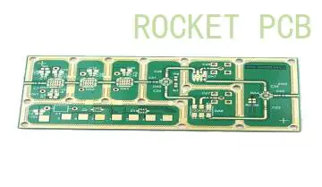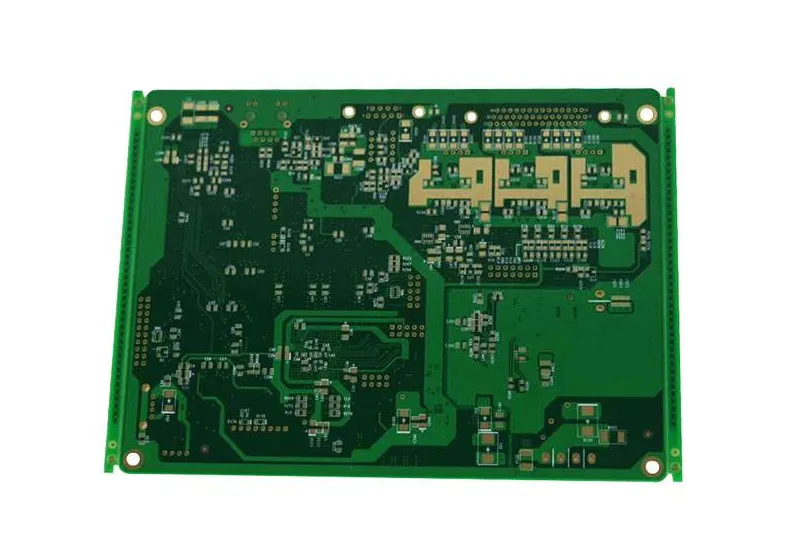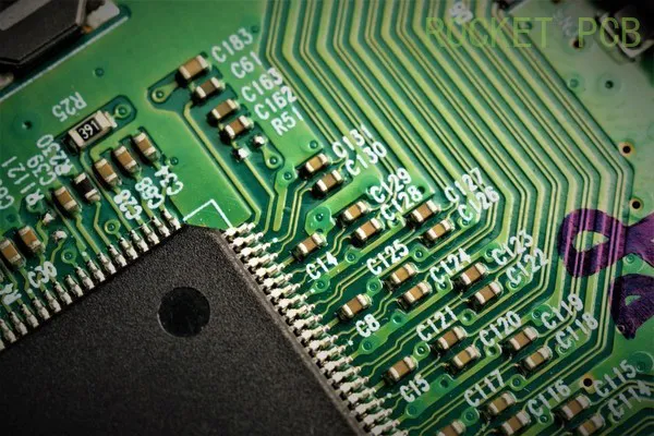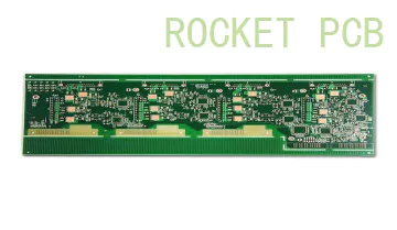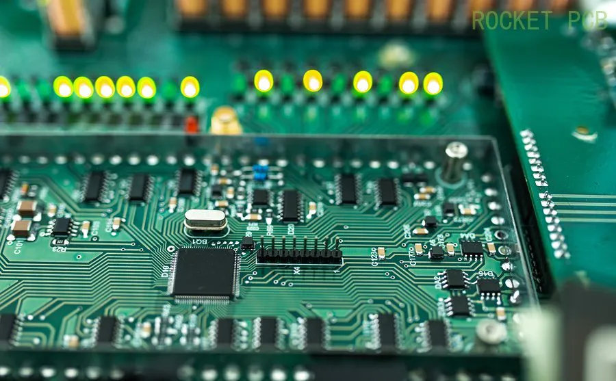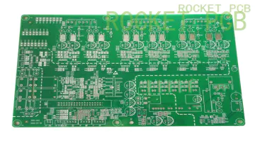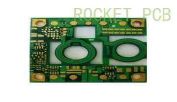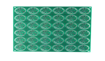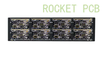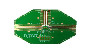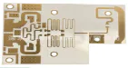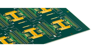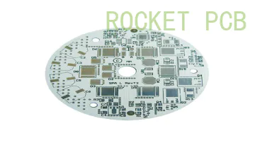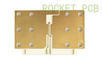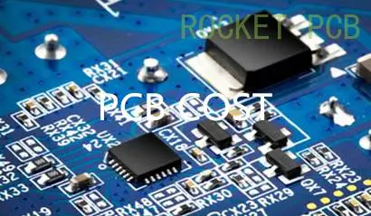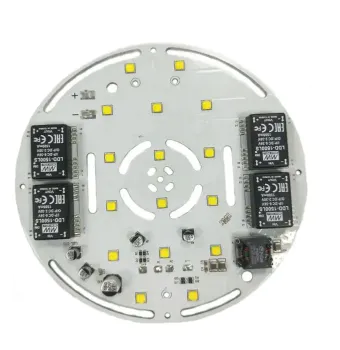


improve your pcb design with these pcb layout tips
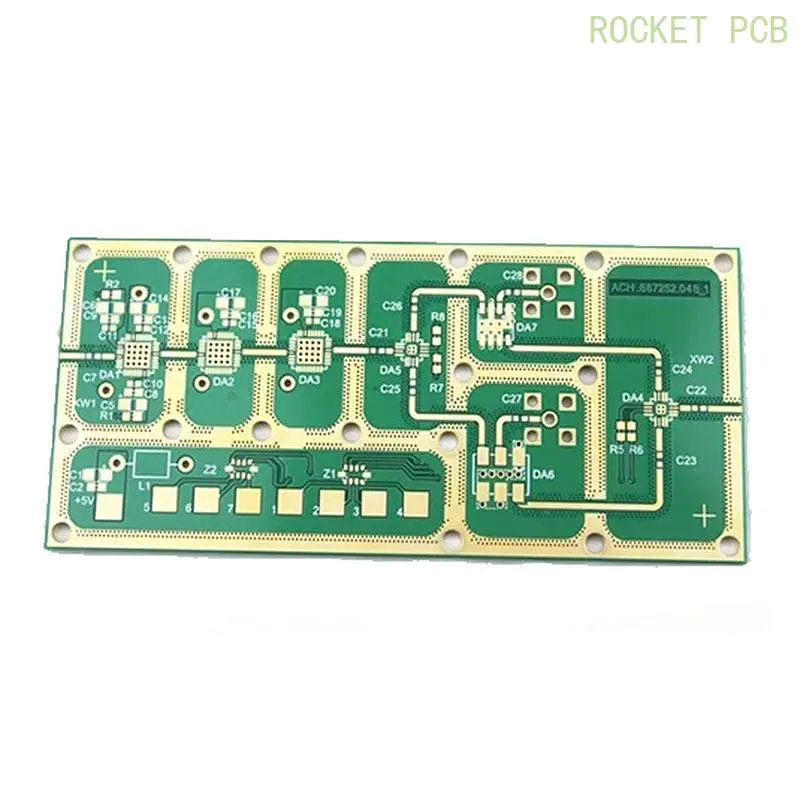
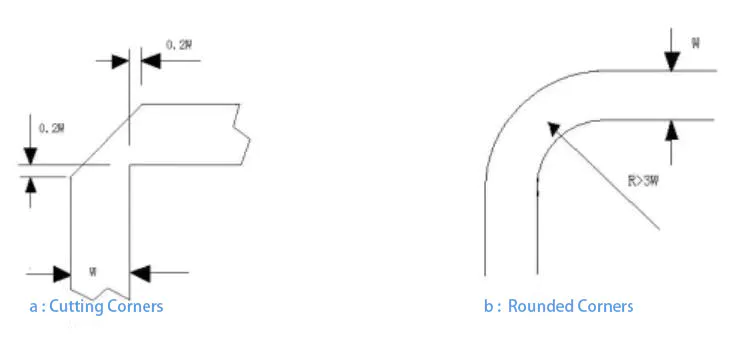
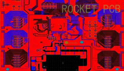
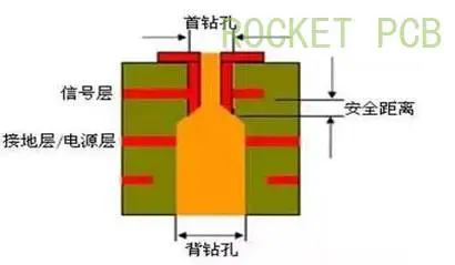
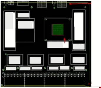
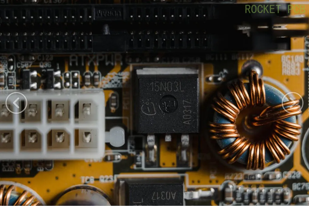
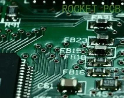
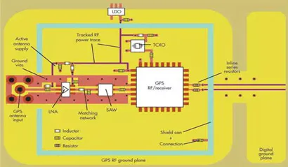
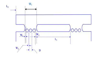
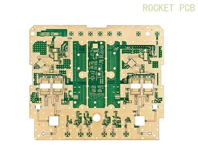
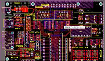
The layout should strive to meet the following requirements: keep the overall wiring as short as possible, with the shortest possible routing for critical signal lines; separate high-voltage, high-current signals from low-current, low-voltage weak signals; separate analog signals from digital signals; separate high-frequency signals from low-frequency signals; and ensure sufficient spacing between high-frequency components.