
loading

BLOG

Why Choose a PCB Prototype Board for Your Project?

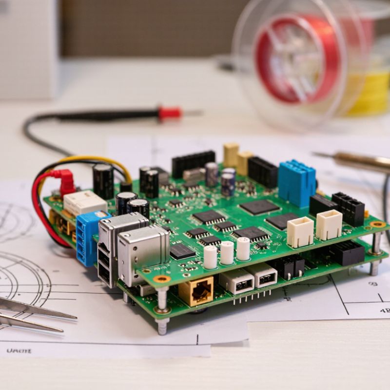
Choosing a Pcb Prototype Board can turn an uncertain circuit concept into something engineers can test with their hands. Instead of trusting a schematic alone, a team can inspect component placement, wiring paths, solder joints, and connector access on a physical board. A small prototype may reveal a reversed pin, an unreachable test point, or unexpected heat near a voltage regulator.

In practical development, this early visibility saves time and limits expensive redesigns. Engineers can measure voltage, current, signal noise, and temperature before approving a production layout. They can also compare the board against component datasheets, design rules, and relevant IPC guidance. Good documentation matters. Record the board revision, materials, test conditions, and every modification.

The details matter.

A reliable Pcb Prototype Board should match the project’s electrical and mechanical requirements. Board thickness, copper weight, layer count, hole size, and surface finish can affect performance. High-speed circuits need controlled routing and careful grounding, while simple control boards may benefit from flexible access points.

Still, a prototype is not proof of final reliability. That assumption can fail. Hand-soldered joints may hide manufacturing weaknesses, and temporary wires can create misleading results. Review the design with experienced engineers, test under realistic loads, and repeat critical measurements. A prototype board works best as a learning tool, not merely a cheaper production board. Its value comes from exposing problems while changes remain practical, affordable, and properly documented.
Why Choose a PCB Prototype Board for Your Project?

What Is a PCB Prototype Board?

Why Choose a PCB Prototype Board for Your Project?

What Is a PCB Prototype Board?

A PCB prototype board is a temporary physical version of an electronic circuit. It converts a schematic into copper traces, drilled holes, pads, and mounted components. Unlike a solderless breadboard, it represents the intended routing and electrical connections more realistically. Most boards use fiberglass material with copper layers, although simple projects may use perforated boards. This physical format exposes spacing, polarity, connector placement, and heat concerns early.

Engineers use prototype boards to test whether a design works beyond computer simulation. A small controller board might include resistors, sensors, headers, and a power circuit on one compact surface. After assembly, technicians check continuity, voltage levels, signal behavior, and component temperature. A mistake becomes visible. A lifted pad, crowded connector, or noisy signal can guide the next revision. In practical development, clear labeling and accessible test points often save more time than extra features.

A prototype board is not automatically production-ready. Its trace width, material, solder mask, and mechanical tolerances may need further review. A circuit can pass bench tests yet fail after vibration or repeated power cycling. That uncomfortable gap deserves attention. Designers should record test conditions, revisions, measurements, and unresolved behavior. The board then becomes reliable engineering evidence, not merely a working demonstration.
How PCB Prototype Boards Support Early Project Development

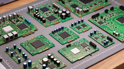
A PCB prototype board gives engineers a practical way to test ideas during early project development. Components can be placed, connected, and adjusted without committing to a final production layout. This hands-on process reveals wiring errors, unstable power connections, and awkward component positions. A schematic may look correct. The board may disagree. That difference matters.

Prototype work also supports measured decisions. Engineers can check voltage rails, inspect signal paths, and observe heat around active components. Experienced developers record test results before changing the circuit. This creates useful evidence for each revision and improves technical reliability. Still, a prototype is not a final product. Temporary connections can fail, while manual wiring may hide design weaknesses. That is a genuine limitation. Treat every test as evidence, not proof.

Tips:

Keep a written pin map beside the board. Label test points clearly. Measure before changing anything. Photograph each revision for comparison. Leave room for mistakes. A small design change can affect the entire circuit, so review power, grounding, and component spacing after every adjustment.

Key Advantages of Using a PCB Prototype Board

Why Choose a PCB Prototype Board for Your Project?

A PCB prototype board turns an electronic concept into something you can touch, test, and improve. In hands-on development, it reveals wiring mistakes that simulations may overlook. You can check component placement, connector access, and enclosure fit before ordering production boards. This early feedback saves time and reduces expensive redesigns.

The main advantage is controlled validation. A prototype board supports testing for voltage stability, signal behavior, heat, and mechanical clearance. Engineers can replace parts, adjust traces, and compare circuit versions quickly. It also improves communication because teams can inspect the same physical device. A visible board often exposes problems faster than a schematic. Still, a prototype is not a finished product. Its routing may be imperfect, and temporary fixes can hide deeper issues.

Tips: Label test points clearly. Keep sensitive signals short. Leave space around hot components. Record every change. Test under realistic loads, not only ideal conditions. If the board works once, that proves very little. Repeated testing matters. Also, review grounding and return paths before blaming individual components. A rushed prototype can create false confidence, but careful iteration builds reliable evidence.

How to Select the Right PCB Prototype Board

Why Choose a PCB Prototype Board for Your Project?

A PCB prototype board lets you test circuit ideas before committing to full production. It exposes wiring errors, thermal issues, and weak connections early. In practical workshops, this can save both materials and troubleshooting time. However, selecting the right board requires more than checking its price.

Match the board to your circuit’s requirements. Choose the correct size, copper layer count, hole spacing, and pad layout. For simple control circuits, a single-sided board may be sufficient. High-speed or densely routed designs usually need better grounding and tighter manufacturing tolerances. Consider the operating current, signal frequency, component package, and expected heat. A board with poor solderability can create unreliable joints. I once selected a convenient board with unsuitable spacing. Reworking it took longer than expected. That mistake still influences my design checks.

Tips: Compare the prototype board with your schematic and component datasheets. Confirm drill sizes before ordering. Inspect the surface for oxidation, scratches, or uneven pads. Leave space for test points and measurement probes. If the project may change, choose a layout that supports easy modification. Keep clear assembly notes. They improve repeatability. Also, do not ignore the enclosure. A board can work electrically and still fail mechanically. Reviewing these details with an experienced technician adds valuable perspective, although even careful reviews can miss one small issue.

Common Applications and Limitations of PCB Prototype Boards

Why Choose a PCB Prototype Board for Your Project?

Common Applications and Limitations of PCB Prototype Boards

PCB prototype boards suit early testing, classroom projects, sensor nodes, LED controls, and small robotics systems. Engineers can place components, adjust wiring, and inspect signals without ordering a finished board. That speed matters. The World Semiconductor Commerce Statistics forecast global semiconductor sales at 611 billion dollars in 2024, showing how quickly electronic designs continue to evolve. Prototype boards help teams respond before committing to production tooling.

They work well for low-frequency circuits, simple power supplies, and proof-of-concept controllers. In bench testing, I find their visible wiring useful for finding reversed diodes or loose ground connections. However, the layout can become crowded quickly. Long jumper wires add resistance and unwanted inductance. High-speed signals may suffer from reflections, crosstalk, and unstable impedance. The board is not always electrically representative.

Thermal and mechanical limits also deserve attention. A prototype board may not dissipate heat like a manufactured PCB with a copper plane and thermal vias. Solder joints can loosen during vibration. Repeated modifications can damage copper pads. IPC-2221 provides established guidance for spacing, insulation, and conductor design, but a universal prototype board cannot fully reproduce those requirements. That is the catch. Treat test results as directional, not final. A design that works on a quiet workbench may fail inside a metal enclosure or near a motor. My earlier assumption that “working” meant “production-ready” was wrong. EMI testing, thermal checks, and a custom PCB remain necessary.

Chat Online
Chat Online
Leave Your Message inputting...
Thank you for your attention. Please kindly describe your question first, or please send your inquiry to our email sale@pcbledmodule.com, and we will reply to you ASAP. Welcome, what can I help you?
Sign in with: