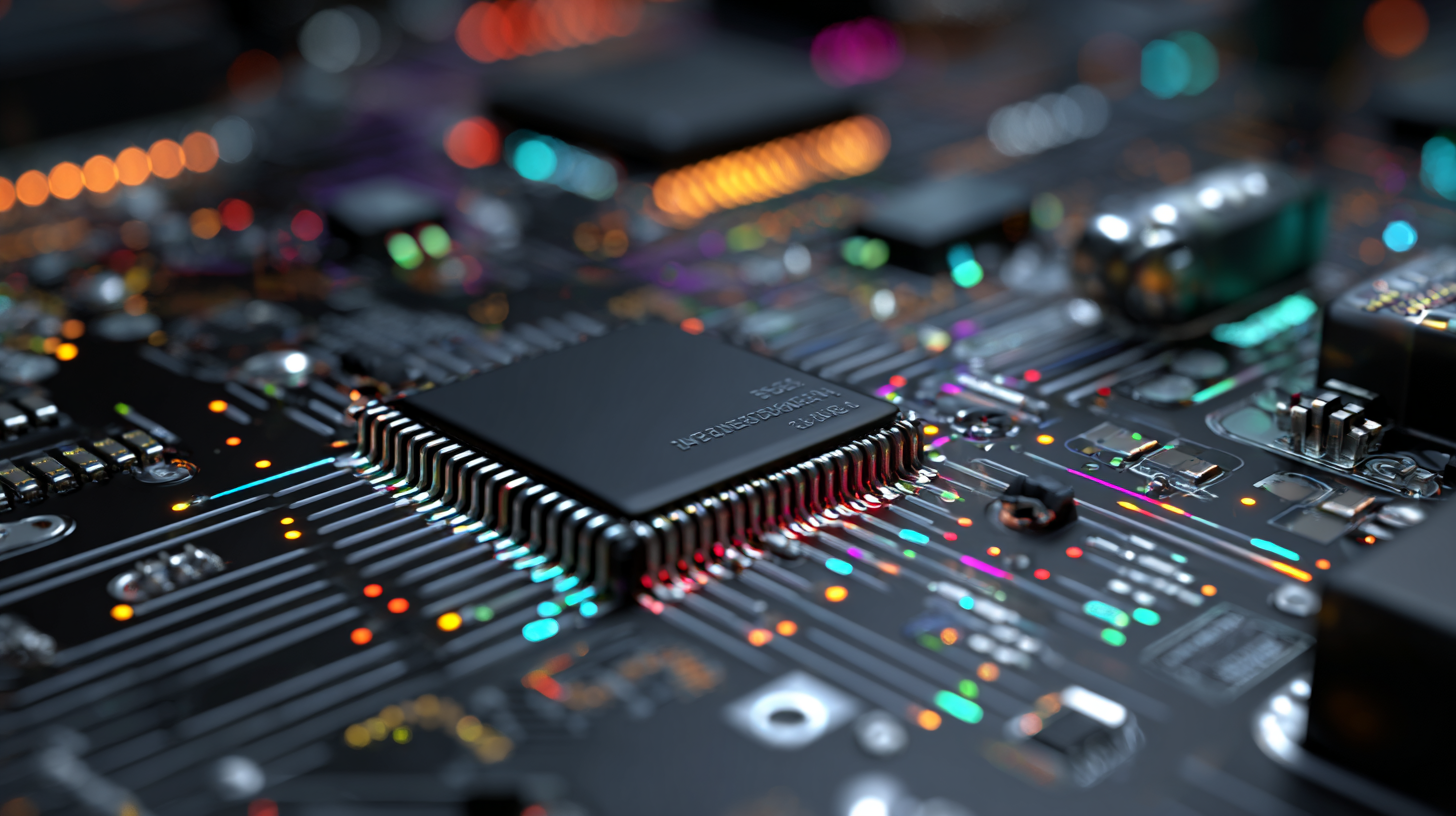
Revolutionizing Electronics: How PCB Circuit Board Innovations Are Shaping Future Designs
The landscape of electronics is undergoing a remarkable transformation, driven largely by innovations in PCB circuit board technology. As the demand for compact, high-performance devices continues to grow, the PCB market is projected to reach $82.9 billion by 2027, increasing at a CAGR of 4.6% from 2020 to 2027, according to a report by Fortune Business Insights. These advancements are not only enhancing the functionality of electronic products but also enabling the integration of emerging technologies such as IoT and AI.
The introduction of flexible PCBs, high-density interconnect (HDI) boards, and environmentally friendly materials signifies a shift towards more efficient and sustainable design practices. As we delve into the fascinating developments in PCB circuit board innovations, it becomes evident that these changes are shaping the future of electronic design, paving the way for smarter and more interconnected devices.
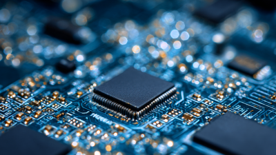
The Impact of High-Frequency PCB Designs on Modern Electronics Performance
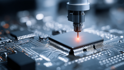
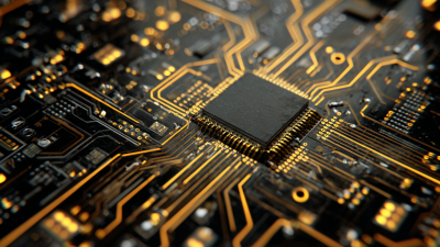
The advent of high-frequency PCB designs is reshaping the landscape of modern electronics, enabling devices to perform with unprecedented efficiency and speed. According to the IPC (Association Connecting Electronics Industries), the market for high-frequency PCBs is projected to grow at a CAGR of 10.5% from 2022 to 2028, driven by advancements in telecommunications, automotive applications, and aerospace technologies. As more devices demand faster data transmission and processing capabilities, engineers are increasingly turning to materials such as PTFE and ceramic substrates, which are specifically engineered for low loss and stable performance at microwave frequencies.
Furthermore, high-frequency PCB designs significantly enhance signal integrity, a critical factor in the performance of modern electronics. A report from Research and Markets highlights that inappropriate PCB layout can lead to issues like signal degradation and crosstalk, particularly at frequencies beyond 1 GHz. Innovations in design software and fabrication methods are addressing these challenges by facilitating tighter spacing of traces and improved shielding techniques. This improvement in design precision not only boosts the reliability of electronic components but also meets the rigorous demands of next-generation wireless communication technologies, such as 5G, which require robust PCB designs for optimal signal propagation and minimal interference.
Revolutionizing Electronics: How PCB Circuit Board Innovations Are Shaping Future Designs - The Impact of High-Frequency PCB Designs on Modern Electronics Performance
| Feature |
High-Frequency PCB |
Standard PCB |
| Signal Integrity |
Excellent |
Moderate |
| Layer Count |
4-20 |
2-10 |
| Material Type |
Low-loss dielectrics |
FR-4 |
| Cost |
Higher |
Lower |
| Applications |
5G, RF, High-speed digital |
Consumer electronics |
Exploring the Role of Flexible PCBs in Next-Gen Consumer Devices
As the demand for next-generation consumer devices escalates, flexible printed circuit boards (PCBs) are emerging as a cornerstone of innovation within the electronics industry. The flexible electronics market is anticipated to expand significantly, with projections indicating a revenue growth from USD 19.92 billion in 2025 to an astonishing USD 83.77 billion by 2034. This surge is driven by the increasing adoption of flexible PCBs in applications such as wearables, sensors, and monitoring devices, where adaptability and miniaturization are paramount.
Moreover, advancements in materials science are contributing to this evolution. Recent breakthroughs have introduced new materials that enable the development of transparent and flexible electronics, pushing the boundaries of what devices can achieve. This aligns with a broader trend in the conductive ink market, which is expected to reach USD 6.96 billion by 2034, reflecting heightened interest in printed electronics that seamlessly integrate with flexible substrates. The integration of these technologies not only enhances device functionality but also underscores the vital role of sustainable practices, paving the way towards a circular economy in electronic design.
The Shift Towards Eco-Friendly PCB Manufacturing Processes and Materials
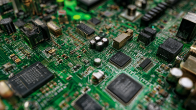
The push towards eco-friendly PCB manufacturing processes is reshaping the electronics industry, driving innovation and sustainability hand in hand. Manufacturers are increasingly adopting materials that are less harmful to the environment, such as biodegradable substrates and non-toxic inks. By utilizing these sustainable resources, companies not only reduce their ecological footprint but also comply with stringent regulations regarding hazardous materials, which are becoming more prevalent worldwide.
Additionally, advancements in recycling technologies are enabling the efficient recovery of valuable components from used circuit boards. This not only conserves raw materials but also mitigates the environmental impact caused by e-waste. The integration of eco-conscious practices in the PCB manufacturing process encourages a circular economy, where materials can be reused and repurposed, ultimately leading to a more sustainable future for the electronics sector. As consumers become more aware of environmental issues, their demand for greener products is motivating manufacturers to innovate and adapt, ensuring that eco-friendly solutions are at the forefront of PCB design and production.
Revolutionizing PCB Manufacturing: Eco-Friendly Innovations
Innovations in PCB Miniaturization and Their Influence on Product Size
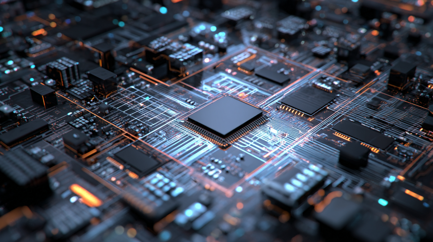
The trend of PCB miniaturization is transforming the landscape of electronics, allowing designers to create more compact and efficient products. According to a recent report from the IPC (Association Connecting Electronics Industries), the global PCB market is expected to reach $82 billion by 2025, driven significantly by the demand for smaller and more powerful devices. This miniaturization is not merely about reducing size but also enhancing performance, enabling advanced features such as higher signal speeds and greater power efficiency.
As manufacturers aim to meet consumer demands for slimmer devices, innovations in materials and design techniques are at the forefront. For example, advancements in flexible printed circuit boards (FPCBs) allow for remarkable space-saving designs, which can lead to reductions in product size by up to 50%. These innovations are particularly crucial in mobile technology, wearables, and IoT devices where size constraints and performance are paramount.
**Tips:** When designing PCBs for miniaturized products, consider using multilayer configurations to optimize space. Additionally, incorporating surface mount technology (SMT) can further reduce the footprint of components. Always stay updated with industry trends and emerging materials to ensure your designs remain competitive in this rapidly evolving market.
Understanding the Importance of Thermal Management in Advanced PCB Design
Thermal management is becoming increasingly crucial in advanced PCB design, especially as electronic systems evolve to meet the demands of modern applications. As military technology pushes the boundaries of performance, effective thermal solutions are required to handle the rising heat levels. This includes not only hardware innovations like heat sinks and liquid cooling systems but also the development of advanced thermal interface materials that facilitate passive heat dissipation. These materials play an essential role in connecting heat-generating components with their heat sinks, thereby enhancing overall efficiency and reliability.

In the automotive sector, similarly advanced thermal management strategies are essential as the demand for high-performance printed circuit boards (PCBs) grows. The anticipated expansion of the automotive PCB market highlights the increasing emphasis on efficient thermal solutions to support electric vehicle technologies and high-power electronics. Innovations such as 3D semiconductor packaging techniques and improved cooling methods are paving the way for more effective systems that can better dissipate heat, ensuring the robust operation of complex electronic devices in critical applications. As these advancements continue, thermal management will remain a focal point in the design and functionality of future electronic circuits.