
English


A Flexible Pcb Board is a thin electronic circuit that bends, folds, or fits around tight spaces. Unlike a rigid board, it uses flexible films, commonly polyimide, instead of conventional fiberglass laminates. Copper traces are patterned onto the film, then protected with coverlay or flexible solder mask. The result feels almost like a narrow ribbon, yet it can carry power and high-speed signals.
Its operation is straightforward. Copper pathways connect components across a moving or irregular assembly. In a smartphone hinge, for example, the circuit can flex repeatedly while maintaining electrical continuity. Bend radius, copper type, layer count, and adhesive selection determine reliability. A smaller radius increases mechanical stress. That detail is often underestimated.
Industry research supports this growing role. IDTechEx, in its Flexible Electronics 2024–2034 report, identifies wearables, medical devices, displays, and automotive systems as major application areas. Grand View Research also reports strong expansion in the flexible electronics market, driven by lightweight products and compact electronic designs. IPC technology roadmaps emphasize miniaturization, signal integrity, material control, and manufacturing consistency as continuing industry priorities.
Still, flexible does not mean indestructible. Repeated sharp bending can damage copper traces. Heat, moisture, and poor strain relief can accelerate failure. Engineers therefore test flex cycles, thermal exposure, insulation resistance, and dimensional stability before approving production. Practical experience matters here. A design may pass electrical tests but fail after thousands of bends. This is why manufacturers must evaluate both the circuit and its installation environment. The technology is powerful, but not magically forgiving.
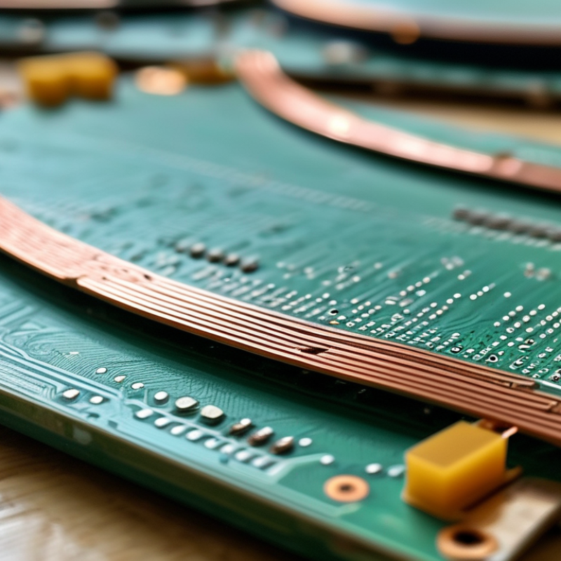
A flexible PCB board is a circuit board that can bend, fold, or fit around shaped components. Unlike rigid boards, it uses a thin, flexible insulating film as its foundation. Copper traces are bonded to this film, while a protective coverlay shields the conductive paths from moisture, dust, and accidental contact. Some designs use several layers for denser wiring.
The board works by carrying electrical signals through these copper traces, just like a rigid circuit board. Its flexible structure allows connections to move with hinges, rotating parts, or compact enclosures. A bend radius matters greatly. If the board bends too sharply, copper traces may develop tiny cracks. They might not fail immediately. This makes inspection more difficult.
In practical assembly work, I have seen flexible circuits solve space problems that cables could not handle neatly. They can reduce connectors, wiring weight, and installation time. However, flexibility does not mean unlimited movement. Repeated bending, heat, sharp edges, and poor support can shorten service life. The design is elegant, but not forgiving. Engineers normally define bend zones, stiffened areas, and suitable copper patterns before production. Testing should include repeated movement and temperature changes. Small details matter.
| Data Dimension | Typical Data or Range | How It Relates to Flexible PCB Operation |
|---|---|---|
| Basic Definition | A circuit board built on a bendable insulating substrate | A flexible printed circuit board electrically connects components while allowing the circuit to bend, fold, or fit into compact three-dimensional assemblies. |
| Primary Substrate | Polyimide film is commonly used | Polyimide provides electrical insulation, dimensional stability, and resistance to elevated processing and operating temperatures. Other flexible dielectric films may be selected for specific designs. |
| Conductive Layer | Rolled-annealed or electrodeposited copper | Copper forms the conductive traces that carry power and signals. Rolled-annealed copper is often preferred where repeated dynamic flexing is required because it has good ductility. |
| Common Layer Configurations | Single-sided, double-sided, and multilayer | Single-sided circuits have one copper layer, double-sided circuits have copper on both sides, and multilayer constructions use additional dielectric and copper layers to increase routing density. |
| Typical Finished Thickness | Approximately 0.05–0.30 mm for many flexible circuits | Actual thickness depends on copper weight, dielectric thickness, coverlay, stiffeners, and the number of conductive layers. Thinner constructions generally improve flexibility but may require additional mechanical support. |
| Minimum Bend Radius | Often about 6–10 times the finished thickness for static bends | The bend radius must be selected from the material stack-up and bend type. Repeated dynamic flexing normally requires a larger radius than a one-time installation bend. |
| Dynamic Flexing | Designed for repeated movement when the stack-up supports it | Dynamic applications require appropriate copper, bend radius, trace geometry, and strain relief. Components, vias, and plated features are normally kept away from the primary flexing zone. |
| Static Flexing | Bent during assembly and then held in position | Static-flex circuits are commonly shaped once to fit a product enclosure. Their design requirements are usually less demanding than those of circuits that flex continuously during operation. |
| Signal Transmission | Electrical signals travel through patterned copper traces | The flexible board works like a rigid PCB electrically. Trace width, spacing, dielectric thickness, copper thickness, and routing geometry determine resistance, capacitance, and signal integrity. |
| Insulation and Protection | Coverlay or flexible solder mask | The protective layer covers exposed conductors, helps prevent short circuits, and improves resistance to handling, moisture, and environmental contamination. |
| Mechanical Reinforcement | Localized stiffeners may be added | Stiffeners made from materials such as polyimide or rigid laminate can support connectors, component areas, and insertion points without making the entire circuit rigid. |
| Thermal Capability | Determined by the dielectric, copper, adhesive, and assembly process | The practical temperature limit is controlled by the complete material system rather than the substrate alone. Component ratings, soldering conditions, and thermal cycling must also be considered. |
| Space-Saving Function | Supports folded and three-dimensional routing | A flexible PCB can replace multiple wired connections and reduce the space, weight, and assembly complexity associated with separate cables and connectors. |
| Typical Applications | Cameras, displays, sensors, medical instruments, automotive modules, and compact electronics | These applications benefit from lightweight interconnections, tight packaging, controlled cable paths, and the ability to accommodate movement or limited installation space. |
| Manufacturing Sequence | Material preparation → circuit imaging → etching → drilling or laser processing → coverlay → plating and finishing → inspection | The process creates the copper pattern, forms interconnections between layers when required, protects the circuit, and verifies dimensional, electrical, and visual requirements. |
| Key Design Constraints | Bend radius, copper grain direction, trace geometry, layer transitions, and strain relief | These factors determine whether the circuit can withstand installation and operation without cracked copper, delamination, conductor fatigue, or electrical failure. |
| Main Advantage | Lightweight, thin, and adaptable interconnection | Flexible PCBs combine electrical performance with mechanical freedom, making them suitable for products where conventional rigid boards or wire harnesses are difficult to install. |
Note: Values shown are common design ranges and general engineering references. Final limits depend on the selected materials, layer stack-up, manufacturing process, bend type, and operating environment.


QUICK LINKS
CONTACT US
Office: (+86) 755 23040566
Tel: (+86) 158 9965 5195
E-mail: sale@pcbledmodule.com
Skype: Hans@Rocket-PCB
Whatsapp: 86 1589965 5195
Office Address: 2207,Bid 4,He Gu Shan Hui Cheng,35#,Guang Tian RoYanluo street, Song Gang Town,518105 SHENZHENG, CHINA
Plant ADD.: No 69, Lianfeng North Road, Xianxi Area, ChangAn Town, Dongguan, China.


Copyright © 2025 Rocket PCB Solution Ltd. | All Rights Reserved Sitemap Friendship link: CNC machining heat sink